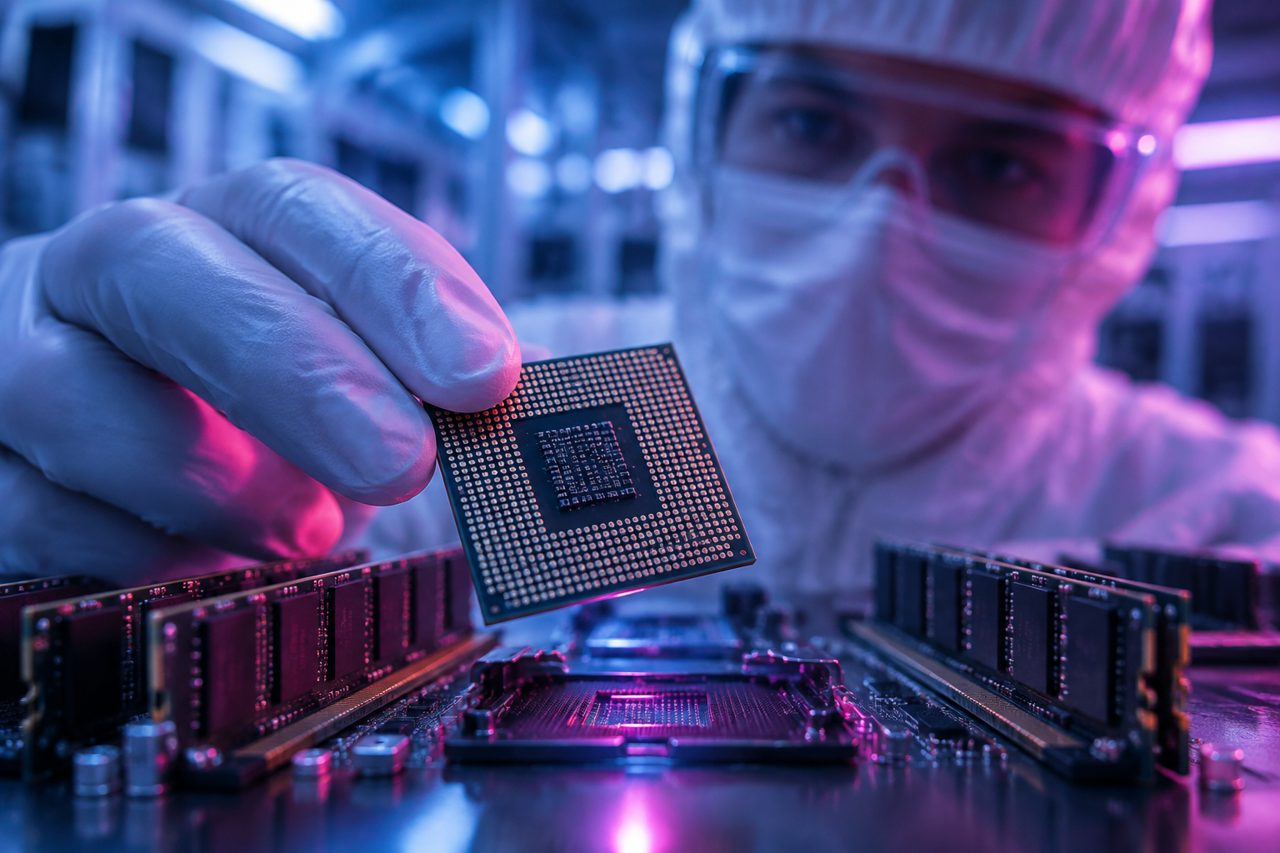
An artificial intelligence chip can have tremendous processing power and still spend some of its time waiting. Waiting for a model’s parameters, waiting for data, waiting for memory to respond. Behind the race for Nvidia and AMD accelerators, another competition has emerged: making memory fast enough and placing it as close as possible to the computing hardware. As of September 2026, understanding this battle requires looking beyond the processor. This analysis draws on established technologies and public announcements, distinguishing future prospects from confirmed facts.
Computing power is no longer everything
In a conventional server, the processor and memory communicate through connections with limited bandwidth. For many applications, that is enough. But large AI models handle vast quantities of parameters and intermediate results. Adding compute units without speeding up their data supply is like expanding a factory without widening its supply routes.
The problem arises during training, when the model learns, but also during inference, when it responds. During text generation, some operations are particularly sensitive to memory read speeds. Other workloads, by contrast, primarily draw on computing power. There is therefore no single bottleneck: it varies with the model’s size, the number of requests and how they are organized.
HBM: a memory tower next to the engine
HBM, short for “High Bandwidth Memory,” addresses this constraint through a different architecture. Multiple layers of DRAM are stacked and linked by vertical connections running through the silicon. These stacks sit close to the processor within the same package. Very wide interfaces allow large amounts of data to move in parallel, with favorable energy efficiency compared with longer connections.
The benefits go beyond bandwidth. Available capacity also determines which models, request batches and context lengths can fit on an accelerator. When data has to be spread further across multiple chips, communication adds complexity and can hurt performance. More memory can therefore avoid some costly transfers.
Announcements in 2024 clearly illustrated this priority. Nvidia introduced Blackwell with HBM3E; AMD unveiled its MI325X, also based on this generation of memory. Behind the performance promises, the industry message was the same: memory is part of the strategic product, not merely an item on a list of interchangeable components.
Packaging becomes a cutting-edge technology
Bringing memory and computing closer together looks simple in a diagram. In a factory, it is a delicate operation. Advanced packaging refers to the assembly and interconnection techniques that allow multiple components to work together. It should not be confused with traditional protective packaging: here, distances, connection density and electrical quality directly influence performance.
TSMC’s CoWoS technology has become emblematic of this shift. Its various versions notably allow processors and HBM stacks to be connected through extremely dense interconnect structures. Not every solution relies on a large, uniform silicon interposer: architectures are evolving to accommodate larger assemblies and keep their costs under better control.
Chiplets reinforce this trend. Rather than always manufacturing a single enormous piece of silicon, designers distribute certain functions across multiple elements. AMD has made this a major strategic focus; the Blackwell GPU announced by Nvidia combines two large compute dies. Packaging must then ensure that communication is fast enough to prevent this physical separation from becoming a disadvantage.
Three memory manufacturers at the heart of the contest
SK hynix, Samsung and Micron occupy a central position in HBM. But producing DRAM is not enough to immediately deliver memory suited to the most demanding accelerators. Manufacturers must master stacking, power consumption, heat and manufacturing consistency, then pass the qualification stages required by customers.
Each generation pushes these requirements further. Stacking more layers increases capacity but complicates manufacturing and heat dissipation. A defect in a component or connection can compromise a high-value assembly. Manufacturing yield therefore becomes as important as advertised performance. Theoretical production capacity does not automatically translate into a volume of qualified products ready for delivery.
The transition to HBM4, set out in industry roadmaps, is also driving closer integration of memory and logic expertise. The growing sophistication of the base die paves the way for closer cooperation with foundries. The prospect is one of more tightly interwoven ecosystems, but their balance will depend on qualification, costs and customers’ actual needs.
An entire supply chain to secure
For Nvidia or AMD, securing chip fabrication capacity therefore does not guarantee delivery of an accelerator. They must also secure memory stacks, advanced assembly, substrates and testing resources. TSMC has begun expanding its CoWoS capacity in response to AI-related demand. Investments by other players also show that assembly is no longer considered a secondary activity.
Yet these links in the chain develop at different speeds. Installing equipment is not enough: processes must be stabilized and teams trained. If memory is in short supply, the processor cannot become a finished product. If packaging capacity is maxed out, available components remain commercially unusable. The bottleneck can thus shift without the pressure easing.
This situation favors long-term commitments and close supplier relationships. Major buyers are better able to anticipate their needs and support investment. For smaller competitors, access to high-performance technology does not necessarily mean rapid access to the volumes they need. Competition plays out as much in industrial planning as in chip design.
The real metric: useful work delivered
For customers, this battle means looking beyond advertised peak performance. Faster or higher-capacity memory can improve a service’s throughput, but only if the software and workload take advantage of it. Reducing numerical precision or compressing models can also ease requirements, with quality trade-offs that need to be assessed.
Cooling matters too: concentrating more computing power and memory makes heat dissipation more difficult. An accelerator’s purchase price therefore tells an incomplete story. For an operator, what matters is the cost of useful work at a given quality and latency, factoring in energy, availability and infrastructure.
What comes next? Competition is likely to continue shifting toward the co-design of computing, memory and interconnects. The next generations of HBM and packaging could boost performance without eliminating the trade-offs between capacity, power consumption and cost. For Nvidia, AMD and their suppliers, winning will not simply mean announcing the best chip: it will mean delivering the best system at scale.