Artificial intelligence chips compute at breathtaking speeds. But they still need to be fed data. Between accelerators, memory and network switches, information travels through infrastructure where every connection consumes power, generates heat and takes up space. Silicon photonics proposes handing some of this traffic over to light. To assess the issues for September 2026, here is what established public developments tell us, and which advances remain prospective.
The challenge is no longer just computation
Training a large AI model involves numerous accelerators exchanging parameters, intermediate results and synchronization data. When one component is waiting for the others, its theoretical processing power is of no use. Inference also faces communication constraints, especially when a model is distributed across several chips. Performance therefore depends on the entire system, not just the processor.
Copper remains excellent over short distances: inexpensive, well understood and easy to integrate. But as data rates increase, signal loss and distortion complicate transmission. Signals need correction, amplification and sometimes regeneration. These operations consume energy and require additional components. The problem becomes particularly acute when hundreds of high-speed links must emerge from a single piece of equipment.
Optical fiber is already ubiquitous in data center networks. The innovation lies in moving electrical-to-optical conversion closer to the circuits that produce the data. Rather than traveling along a long electrical trace before reaching a front-panel optical module, the signal can be converted much earlier.
What silicon photonics actually does
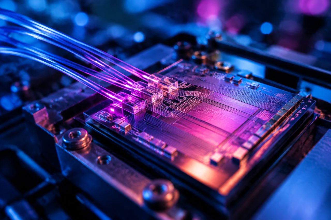
On a photonic chip, waveguides channel light. Modulators encode electrical information onto it, while photodetectors perform the reverse conversion. Several wavelengths can share the same optical path, multiplying the number of channels without a corresponding increase in fibers. Electronics remain essential to drive and receive these signals.
Silicon appeals to manufacturers because it benefits from an extensive manufacturing ecosystem. That does not mean a processor factory can produce all the necessary optical components without adaptation. Processes, materials and testing requirements differ. Above all, silicon is a poor light emitter: lasers generally rely on other semiconductors, whether integrated, assembled or positioned remotely.
The aim is therefore not to replace transistors with photons for every operation. In this application, light carries data; electronics continue to perform computations. The distinction matters, because the promises of optical computing and optical interconnects address different challenges.
Bringing optics and processors closer together
The first stage is already in commercial production: pluggable optical modules installed on the front panels of network equipment. They can incorporate silicon photonics and offer a major practical advantage: a technician can replace a faulty module without touching the processor or switch. This modularity explains their resilience in the face of more integrated architectures.
Another approach, known as co-packaged optics, brings optical engines closer to the electronic circuit within the same package. Electrical paths become shorter, potentially reducing their power consumption and making higher data rates easier to achieve. In return, the optics sit next to hot components, in an environment that is more difficult to manufacture, cool and repair.
Public announcements illustrate this progression. In 2024, Intel demonstrated a prototype optical interconnect chiplet co-packaged with a processor. Broadcom has also developed solutions combining network switching and co-packaged optics. Specialists such as Ayar Labs are working on optical input/output. These developments demonstrate a technological direction, not widespread adoption in AI servers.
Energy: a promise that must be measured in the right place
A fiber carries a signal without the same electrical losses as a copper trace. Yet an optical link never comes without an energy cost. The laser, modulation and receiver circuits, and any thermal stabilization devices all need power. Conversions between the electrical and optical domains must also be included in the assessment.
The relevant comparison therefore covers the complete link, at comparable distances and data rates. A measurement limited to the modulator can look impressive without reflecting the system’s actual power consumption. Over a few millimeters, a well-designed electrical connection may remain preferable. Over longer distances, or when connection density becomes a constraint, optics become more attractive.
Another caveat: reducing energy per bit does not guarantee lower total consumption. If operators use that efficiency to increase data exchanges, overall energy use may continue to rise. The benefit would then be greater capacity within a given energy budget, rather than an absolute reduction in consumption.
The real challenge lies on the factory floor
Aligning, assembling, testing
Connecting a fiber to a photonic circuit requires highly precise alignment. A tiny offset can cause losses that require increased optical power. Repeating this assembly process quickly, with high yields and at an acceptable cost, is far more difficult than producing a successful laboratory demonstration.
Testing is a second bottleneck. The industry knows how to test electronic circuits at wafer level on a large scale. Adding optical measurements, checking coupling and characterizing multiple wavelengths makes this stage more complex. Defects must be detected before an expensive part is integrated into an even more expensive assembly. Otherwise, a single faulty element can severely undermine production economics.
Heat and maintenance
Some photonic components are sensitive to temperature changes. An AI accelerator, meanwhile, is an intense and variable heat source. The design must therefore reconcile thermal management, optical stability and mechanical constraints. Active tuning can help, but it consumes energy in turn.
Maintenance also requires a rethink of the architecture. With a pluggable module, replacement is relatively straightforward. With tightly integrated optics, it can become more involved. External, replaceable lasers offer one possible approach, without solving every difficulty. For operators, availability, service life and repairability matter as much as maximum data rates.
A selective transition rather than wholesale replacement
The most plausible trajectory is long-term coexistence. Electrical connections would retain the distances and applications where they remain competitive. Optical modules would continue to connect large numbers of devices. Co-packaged optics would advance first where bandwidth, reach and power consumption justify their additional cost. When assessing announcements, system-level results, manufacturing yields and maintenance requirements are more useful indicators than isolated records.
What comes next? Looking ahead to September 2026 and beyond, the decisive test will be industrial: delivering reliable, reproducible and economically compelling interconnects. If assembly and testing improve, light could move even closer to accelerators. But adoption will probably remain gradual: less a disappearance of copper than an intelligent redistribution of roles between electrons and photons.