On a roof crowded with chimneys or at a space-constrained solar farm, every square metre counts. This is where tandem solar captures the imagination: adding a perovskite layer to silicon to convert more light into electricity without making panels larger. The promise is substantial, backed by rapid progress in the laboratory. But between a record-breaking cell and equipment capable of generating power for several decades lies a demanding industrial journey. Looking ahead to September 2026, the real test is not just efficiency: it is trust.
This analysis draws on scientific findings and industrial developments documented through 2024. The outlook discussed for 2026 consists of projections, not a review of announcements or performance verified as of that date.
Two materials to make better use of light
Silicon dominates photovoltaics because it combines efficiency, stability and mass production. But a conventional cell makes imperfect use of the solar spectrum. Some of the energy carried by higher-energy photons ends up as heat. Process improvements still offer scope for progress, but they do not remove the physical limits of a single-junction cell.
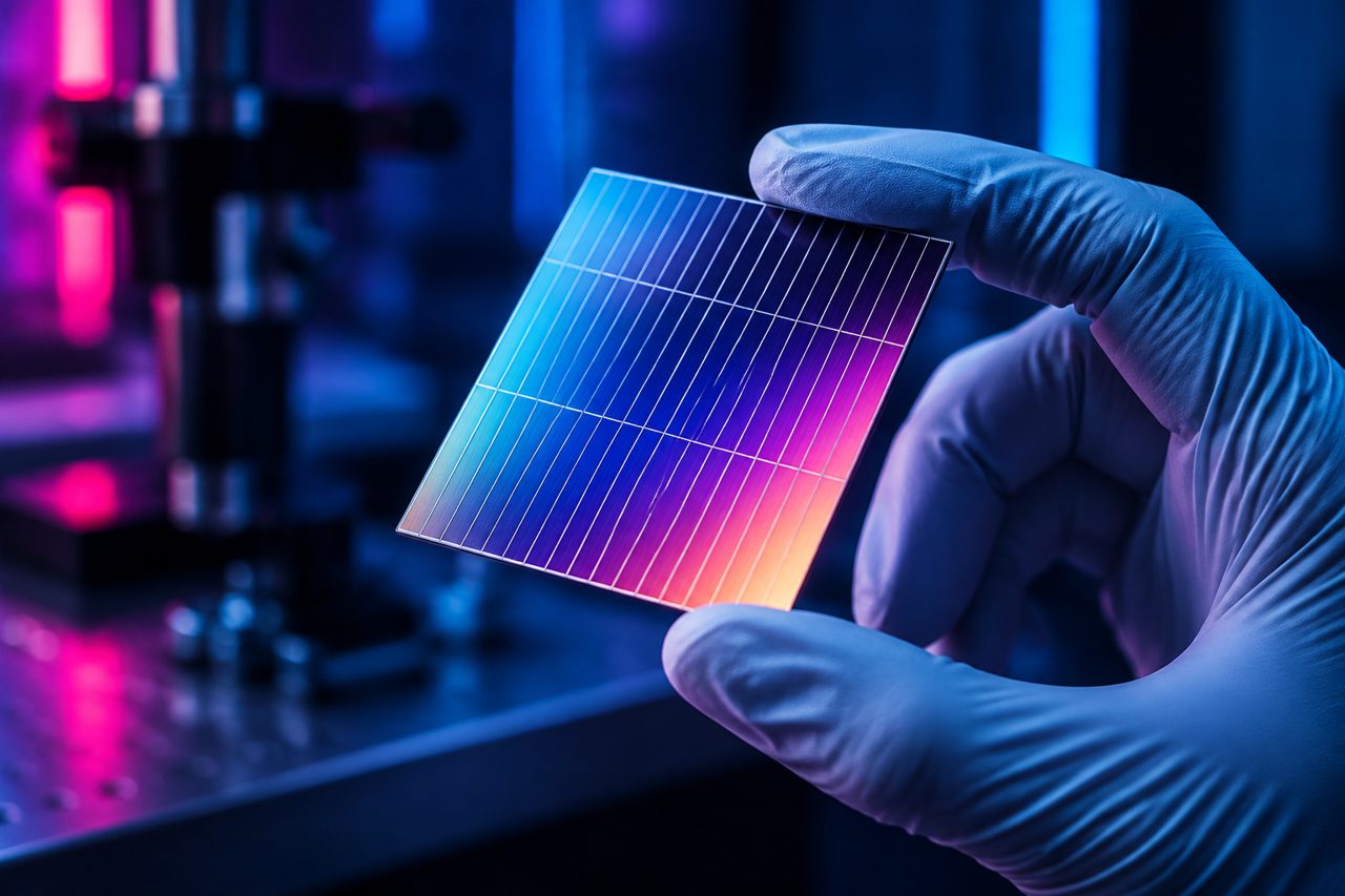
Tandem technology takes a different approach: it stacks two absorbers with complementary properties. On top, a perovskite captures some of the visible light, particularly higher-energy photons. Below, silicon makes greater use of the wavelengths that pass through this first layer. The spectrum is shared more effectively, potentially allowing more of its energy to be harnessed.
Here, “perovskite” refers to a crystal structure, not a single material. The compositions studied for photovoltaics are generally metal halides, often lead-based. Their appeal stems in particular from a valuable property: their bandgap, which determines the light energies they absorb, can be adjusted through their composition.
Impressive records, but not yet lower electricity bills
By 2024, perovskite-silicon tandem cells had already exceeded 34% certified efficiency in the laboratory. This surpasses the performance of the best silicon-only cells and shows that the stacked approach works. The progress is all the more remarkable given how young this technology is compared with silicon’s decades of development.
Care is needed, however, when interpreting what a record measures. It applies to a cell of a given area under standardised conditions. A commercial module incorporates interconnections, borders, glass and various protective materials. These components introduce losses. Larger areas also bring challenges of uniformity: a poorly deposited region can impair the whole device.
The ultimate measure remains the electricity generated over the panel’s entire lifetime. Higher initial efficiency does not guarantee a better investment if power output falls too quickly. Temperature, shading, the light spectrum and the electrical behaviour of the two subcells also matter. In two-terminal architectures, their series connection makes it particularly important to match their currents closely.
Sunlight is also a stress test
The paradox of perovskites is simple: they must endure the very stresses that enable them to generate power. Intense light, heat and electrical voltage can promote internal changes. Moisture and oxygen are other enemies. Depending on the compositions and interfaces, ions migrate, defects emerge and performance deteriorates.
For some wide-bandgap perovskites used in tandem cells, light-induced phase segregation presents an additional challenge. The local composition can change, altering optical and electrical properties. Researchers are therefore working as much on the material’s chemistry as on defect passivation and the layers that extract charge carriers.
Encapsulation is essential, but it is no magic wand. It must limit ingress without weakening the stack, withstand thermal cycling and remain compatible with industrial processes. Edges, seals and interfaces become as important as the active layer. An excellent material with poor protection does not make a good panel.
What accelerated tests alone cannot tell us
Damp-heat, thermal-cycling and light-exposure tests help compare solutions and eliminate certain weaknesses. Passing qualification tests under photovoltaic standards is a necessary step. It does not automatically demonstrate a lifetime of twenty-five or thirty years, especially for a technology with different ageing mechanisms.
Accelerated testing must be combined with physical understanding and long-term outdoor measurements. A hot, dry climate does not place the same stresses on a panel as a humid region or one exposed to freezing conditions. For buyers, the question becomes practical: what losses have been observed, under what conditions, and who will bear the financial cost of excessive degradation?
Manufacturing the same good cell millions of times
Depositing a perovskite layer over a small area is one thing; reproducing it quickly on industrial cells is another. Thickness, crystallisation, purity and freedom from defects must remain under control. Silicon’s textured surfaces, useful for trapping light, make achieving a uniform coating even more difficult.
Several approaches coexist: solution deposition, vacuum processes and hybrid methods. Each involves trade-offs between throughput, material consumption, layer control and capital investment. Solvents, their recovery and operator safety also enter the equation. A recipe that works in the laboratory is not necessarily suited to a continuous production line.
By 2024, companies such as Oxford PV had already begun industrialising perovskite-silicon tandem technology. These efforts give the concept a manufacturing reality, without in themselves demonstrating its competitiveness at very large scale. Manufacturing yield — the proportion of products that meet specifications — will be just as decisive as electrical conversion efficiency.
An innovation up against fiercely competitive silicon
Tandem technology is not competing with a technology that stands still. Silicon cells continue to improve, notably through TOPCon and heterojunction architectures. Above all, their industry benefits from equipment whose costs have already been amortised, established supply chains and enormous production volumes. Pressure on module prices makes any additional cost difficult to justify.
Tandem technology could therefore gain traction first where space is expensive: constrained rooftops, commercial buildings or projects limited by their footprint. More power per panel can reduce certain structural, wiring or installation costs for the same installed capacity. But this benefit will have to offset the higher price and uncertainties over ageing.
Lead adds an environmental requirement. The risk depends in particular on its containment and potential release following breakage. Layers capable of retaining it, collection procedures and appropriate recycling must accompany the product. Promising low-carbon electricity does not remove the need to plan for materials’ end of life.
What next? For 2026 and beyond, the credible scenario is a gradual scale-up rather than a sudden replacement of silicon. The decisive evidence will be reproducible modules, transparent field data, robust warranties and economically viable production. Tandem technology has a genuine physical advantage. It must now demonstrate that this advantage survives the factory, the seasons and the long term.